|
|
|
|
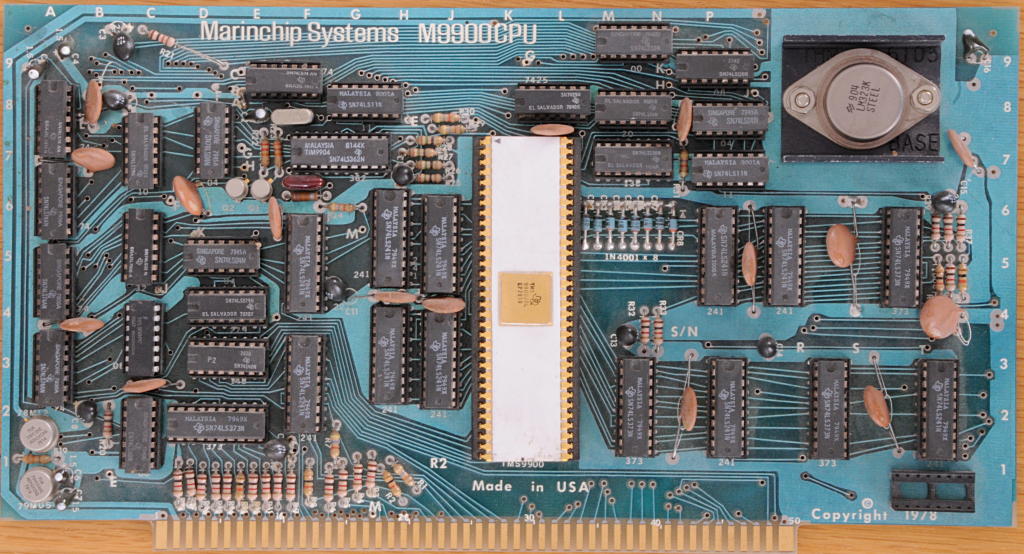
The M9900CPU was Marinchip's first product and was the heart of every system we sold. It was a single S-100 board, designed and laid out by Fred Camerer, which interfaced the 16-bit Texas Instruments TMS9900 microprocessor to the S-100 bus, which was designed for 8-bit processors. It was able to either turn 16-bit memory accesses into sequential pairs of bus requests or, if the memory signaled its ability to run in 16-bit mode, a single 16-bit access which was twice as fast. This protocol was eventually adopted as part of the S-100 standard (IEEE-696). It brought the 9900's “CRU” serial I/O facility out to unused pins on the S-100 bus, allowing it to work with Marinchip's peripherals such as the PROM/RAM/SIO/RTC and Quad SIO boards.
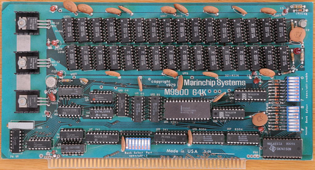
In an era where many personal computers used multiple 8 Kb static RAM boards, which consumed slots in the chassis, lots of power, and emitted abundant heat, the Marinchip M9900 64K was revolutionary, although initially greeted with scepticism by customers. There are two kinds of random access memory (RAM): static and dynamic. A static RAM chip simply stores the data permanently, using multiple transistors per bit (usually four at the time), but requires power regardless of whether the memory is being accessed or not. A dynamic RAM chip needs only one transistor per cell, and hence can store four times the amount of data on the same size silicon chip, but it requires “refresh”. If you don't periodically read the data and write it back, it will “forget” the data and it will be corrupted.
Used properly, and observing the manufacturer's refresh requirements, dynamic RAM chips are perfectly reliable and consume far less power than static RAMs while providing four times the storage density. But, given the general flakiness of the S-100 bus and the peripherals people connected to it, dynamic RAM cards received a well-deserved reputation for unreliability. Everything would be just tickety-boo, and then your “sloppy disc” controller would lock up the bus, refresh would fail, and HAL could only remember the first song he was taught.
The M9900 CPU provided a unique opportunity to exploit the newly-announced 4116 16 K dynamic RAM chips. Just 32 of these chips, fitting easily on an S-100 bus card, would fill the entire 64 Kb address space provided by that bus. Using the M9900 CPU's 16-bit addressing mode, it would run twice as fast as conventional S-100 memory, and by performing all refresh operations on the memory card, completely autonomously to whatever was going on in the computer, rock-solid refresh would be guaranteed (and, just to be sure, I refreshed about ten times as frequently as required, which actually only negligibly increased the power requirements).
This board was originally prototyped on a wire-wrap card, then refined by Fred Camerer, who made the digital design far more elegant and laid out the printed circuit board by hand with red and blue tape. The dynamic RAM chips are tilted because that allows the bus lines which connect them to run straight rather than zig and zag up and down from chip to chip. You'd never do that today, because it would prevent machine-stuffing of the boards, but that wasn't a consideration in the late 1970s.
A single M9900 64K board filled up the entire address space of the M9900 CPU, but not our ambitions. The DIP switch at the bottom allowed you to assign a memory board a “Bank ID”, and the switches at the right allowed disabling parts of the address space to which the board responded. By setting the switches appropriately, you could install as many of these boards in your machine as you had slots available, and configure them so that our NOS/MT operating system could switch among them, providing each user his or her own 64 Kb (less operating system overhead, which was shared), completely isolated from the address space of other users. This wasn't elegant by today's standards of virtual memory and vast flat address spaces, but it got you there, and users were able to configure multi-user systems which shared a large hard disc and met the needs of their businesses.
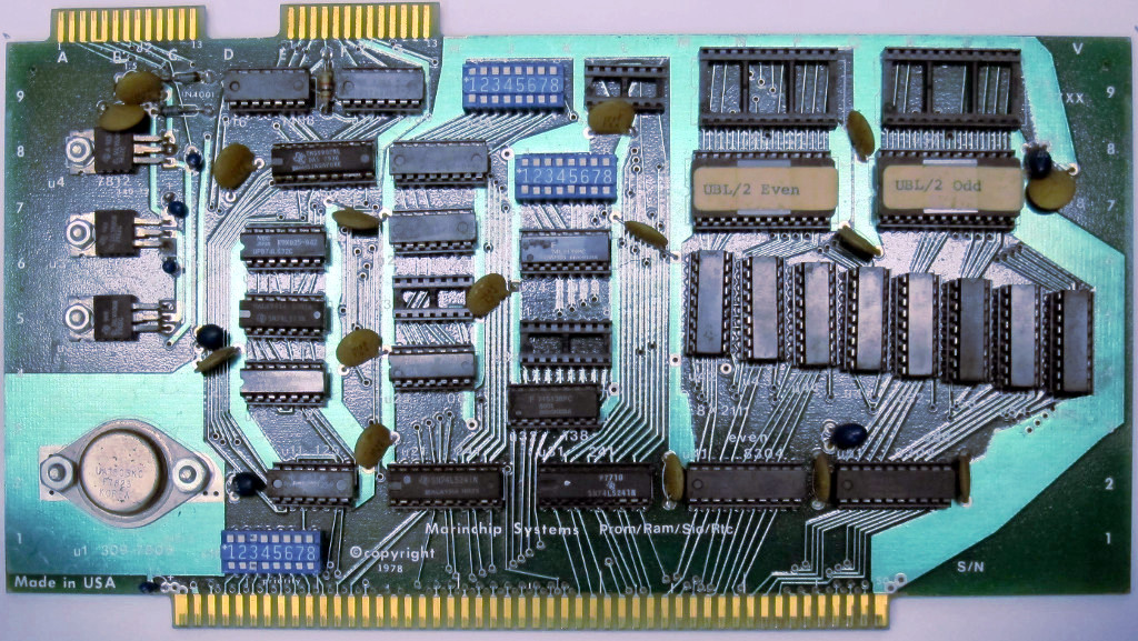
The PROM/RAM/SIO/RTC board provided one serial port (brought out to two connectors at the top, one configured for direct connection to a terminal, the other to a modem—they were wired in parallel and could not be used simultaneously), the 2 Kb PROM monitor, stored in two 2708 UV-EPROMS, 1 Kb of RAM, which was accessed 16 bits wide using the M9900's 16-bit mode (and hence twice as fast as conventional 8-bit S-100 memory), and a real-time clock.
The PROM monitor provided basic debug functions (the ability to inspect and change registers and memory, etc.) and booting the system from a floppy disc. Later versions of the PROM monitor supported booting from the hard discs which were eventually supported.
The PROM/RAM board was not yet available when the M9900 CPU first shipped. Early installations used third-party S-100 PROM and serial port boards. We also briefly sold a version of this board called the Marinchip SIO, which was the same printed circuit populated only with the parts which implement the serial port. This was used to connect serial printers and additional terminals on multi-user systems before the Quad SIO board became available. With the introduction of the Quad SIO, it was discontinued.
This photo was taken by Jim Hearne, and kindly provided by Paul Ruizendaal.
M9900 PROM/RAM/SIO/RTC Theory of Operation and Configuration Guide
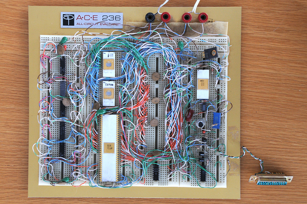
Here's where it all began. Before embarking on the design of the M9900 CPU, I wanted to become familiar with the processor in a much simpler environment, so I wired up this single-board computer on a prototype board. Using it, I developed a PROM monitor (stored in the 2708 chips above the processor), which eventually became the monitor and boot PROM of the PROM/RAM/SIO/RTC board. The system communicated with an ASCII terminal, which was connected to the DB-25 connector at the right. The binding posts at the top connected to an external power supply. Some non-generic chips from this prototype board are missing, having been reused in the wire-wrapped two-board prototype of the M9900 CPU. To the right of the column of chips with the PROMs and TMS9900 CPU were four Intel 2111 256×4 static RAM chips, providing a total of 512 bytes of RAM. The reset button is visible at the right, below the centre. Humorously, the TMS9900 chip I used in this prototype system (with a 1976 date code) was defective: the divide instruction did not work. Today, I'd post a scathing message on my blog and Twitter and await a replacement, but back then I just re-implemented divide with a subroutine that did successive subtractions and soldiered on until I could afford another chip.
|
|